Home
Free Trial
Home
Free Trial
Read More
Content
Filter
10 results found
Featured
Reliability Overview | Allegro X
Featured
ICT vs Flying Probe: Factory Testing of PCB Assemblies
Featured
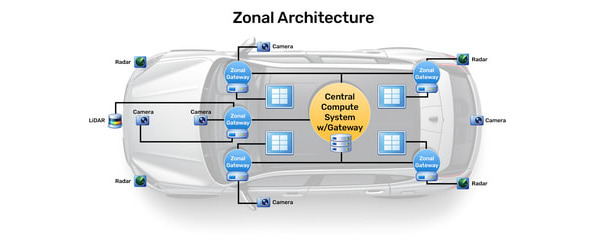
Software-Defined Vehicles: When Timing Becomes a Safety Risk
Featured
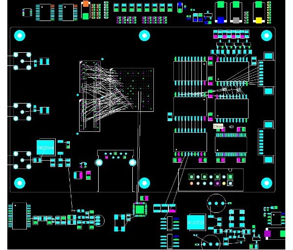
Reviewing The PCB Design Review Process
Featured
PCB Substrates Part 2: A Performance-Driven Approach to Reliability in 2025
Featured
PCB Design Strategies: Designing for High-Pin Count Devices
Featured
Constraint Driven Design in OrCAD X
Featured
Microvia Reliability in High-Density Designs
Featured
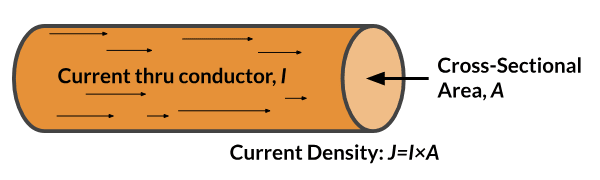
Copper Current Density in PCB Design
Featured
High Voltage PCB Design Guidelines
Featured
Products
None
Allegro X PCB
(2)
OrCAD X
(2)
Content types
None
Video
(1)
Blog
(7)
Design Guide
(1)
Solutions
None
Design for Reliability
(3)
Schematic Capture
(1)
Constraint Management
(1)
Video is muted due to browser restrictions. Adjust the volume on the video player to unmute.
Close
Selected language is not available in captions.
Close