Home
Free Trial
Home
Free Trial
Read More
Content
Filter
10 results found
Featured
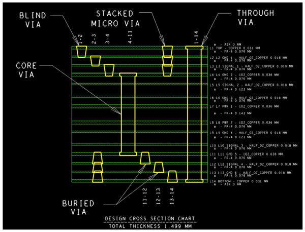
An Introduction to Microvias in PCB Design
Featured
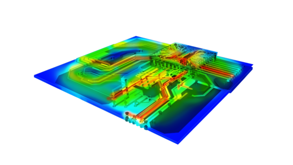
Navigating Signal Integrity Challenges in High-Speed PCB Design: Practical Tips to Solve Common Obstacles
Featured
Grounding and Return Paths: Advanced Techniques - Part Two
Featured
Grounding and Return Paths: Essential for High-Speed Designs - Part 1
Featured
Differential Pairs: From Basic Concepts to Advanced PCB Routing
Featured
OrCAD X High-Speed Digital Design Guide Part 2
Featured
OrCAD X High-Speed Digital Design Guide Part 3
Featured
How to Reduce EMI in Your PCB Design Using Grounding and Via Shielding
Featured
How to Import and Place 3D Mechanical EMI Shielding Model in Your PCB Design
Featured
How to Reduce EMI in Your PCB Design Using Return Path Constraints
Featured
Products
None
OrCAD X
(5)
Content types
None
Blog
(5)
Design Guide
(2)
Video
(3)
Solutions
None
Thumbnails
Document Outline
Attachments
Layers
Current Outline Item
Previous
Next
Highlight All
Match Case
Match Diacritics
Whole Words
Color
Size
Color
Thickness
Opacity
Presentation Mode
Open
Print
Download
Current View
Go to First Page
Go to Last Page
Rotate Clockwise
Rotate Counterclockwise
Text Selection Tool
Hand Tool
Page Scrolling
Vertical Scrolling
Horizontal Scrolling
Wrapped Scrolling
No Spreads
Odd Spreads
Even Spreads
Document Properties…
Toggle Sidebar
Find
Previous
Next
Presentation Mode
Open
Print
Print
Download
Download
Current View
FreeText Annotation
Ink Annotation
Tools
Zoom Out
Zoom In
Automatic Zoom
Actual Size
Page Fit
Page Width
50%
75%
100%
125%
150%
200%
300%
400%
More Information
Less Information
Close
Enter the password to open this PDF file:
Cancel
OK
File name:
-
File size:
-
Title:
-
Author:
-
Subject:
-
Keywords:
-
Creation Date:
-
Modification Date:
-
Creator:
-
PDF Producer:
-
PDF Version:
-
Page Count:
-
Page Size:
-
Fast Web View:
-
Close
Preparing document for printing…
0%
Cancel