Home
Free Trial
Home
Free Trial
Read More
Content
Filter
10 results found
Featured
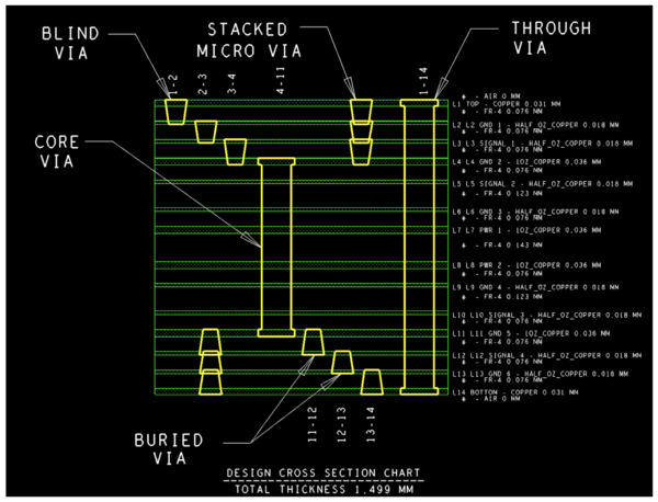
An Introduction to Microvias in PCB Design
Featured
Navigating Signal Integrity Challenges in High-Speed PCB Design: Practical Tips to Solve Common Obstacles
Featured
Grounding and Return Paths: Advanced Techniques - Part Two
Featured
Grounding and Return Paths: Essential for High-Speed Designs - Part 1
Featured
Differential Pairs: From Basic Concepts to Advanced PCB Routing
Featured
OrCAD X High-Speed Digital Design Guide Part 2
Featured
OrCAD X High-Speed Digital Design Guide Part 3
Featured
How to Reduce EMI in Your PCB Design Using Grounding and Via Shielding
Featured
How to Import and Place 3D Mechanical EMI Shielding Model in Your PCB Design
Featured
How to Reduce EMI in Your PCB Design Using Return Path Constraints
Featured
Products
None
OrCAD X
(5)
Content types
None
Blog
(5)
Design Guide
(2)
Video
(3)
Solutions
None