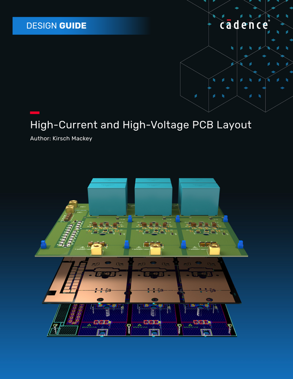
Learn PCB layout best practices for high-current and high-voltage designs, including trace sizing, via current distribution, thermal bottlenecks, and creepage clearance.
Fill This Out to Continue
This content will be available after you complete this form.