Design Guides


Navigate complex PCB design and analysis challenges with our expert design guides. These resources offer step-by-step instructions, practical advice, and proven techniques to enhance your skills.
Sample content thumbnail
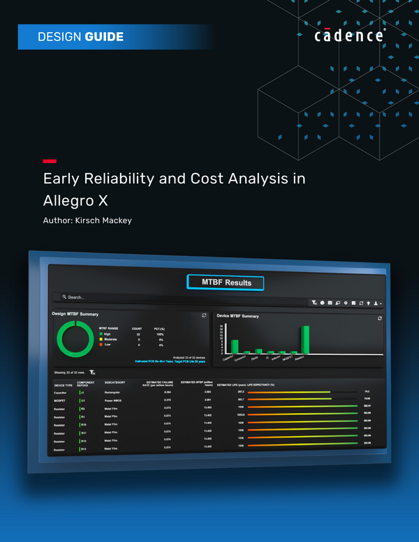
Early Reliability and Cost Analysis in Allegro X
Learn how front-end reliability analysis in Allegro X System Capture reduces board spins, lowers development costs, and protects margins by evaluating electrical stress, derating, and product life directly within the schematic environment.
View Now
Sample content thumbnail
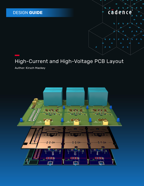
High-Current and High-Voltage PCB Layout
Learn PCB layout best practices for high-current and high-voltage designs, including trace sizing, via current distribution, thermal bottlenecks, and creepage clearance.
View Now
Sample content thumbnail
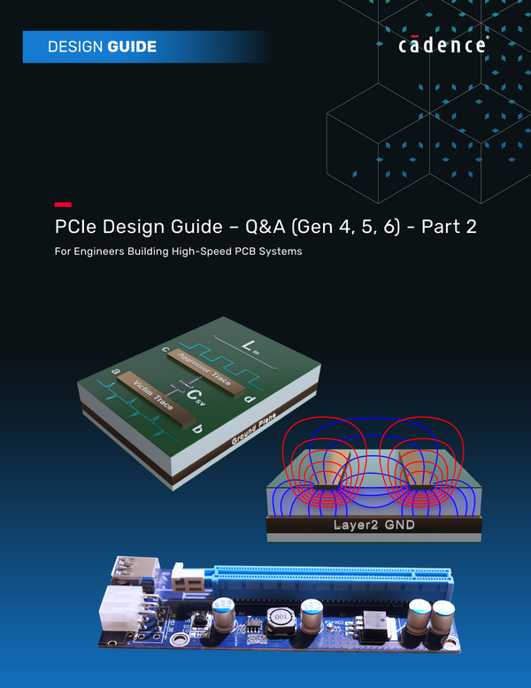
PCIe Design Guide – Q&A (Gen 4, 5, 6) - Part 2
Learn advanced PCIe design techniques with expert guidance on simulation, validation, signal integrity, power integrity, PAM4, and Gen6 compliance.
View Now
Sample content thumbnail
PCIe Design Guide – Q&A (Gen 4, 5, 6) - Part 1
Explore 60 expert Q&As on PCIe Gen4, Gen5, and Gen6 PCB design, covering routing, stackup, signal loss, equalization, and compliance best practices.
View Now
Sample content thumbnail
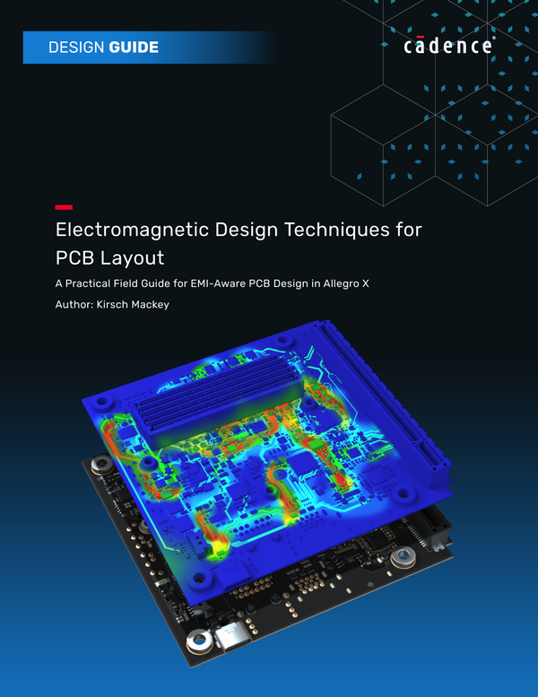
Electromagnetic Design Techniques for PCB Layout
Learn PCB layout techniques that prevent EMI failures before compliance testing. Covers stackup, return paths, decoupling, and Cadence Allegro X workflow.
View Now
Sample content thumbnail
Differential Pair Routing for Signal Integrity and EMI
Route high-speed differential pairs with better signal integrity and lower EMI. Learn stackups, impedance control, Allegro X constraints, routing, via design, and fixes for skew and crosstalk.
View Now
6 results found