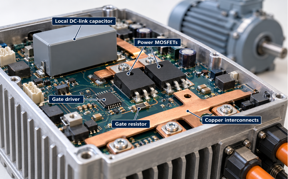
Inside the inverter. The local DC-link capacitor supplies rapidly changing switching current. The gate driver and gate resistor control the MOSFET gates. Copper interconnects carry current between components and add inductance. Conceptual illustration; component placement is illustrative. Figures 1 and 2 show the electrical paths.
Your inverter schematic can be correct, yet the physical bench build might still suffer from voltage spikes, gate ringing, or excessive power loss. PCB traces and transistor packages add inductance, and nearby conductors can couple electrical disturbances into each other. To track down these issues, start by mapping the power commutation loop. Then trace the gate-driver path and locate any source connection shared by gate current and power current.
Key takeaways
- When current transfers quickly between switching paths, power-loop inductance produces a voltage that can add to the transistor’s drain-to-source voltage.
- Gate-loop inductance and shared source inductance can disturb gate-to-source voltage. A large enough disturbance can turn on a device that should remain off.
- Adjusting gate resistance alters switching delays; always re-verify half-bridge dead time to protect your DC rails.
Why Fast Switching Causes Voltage Spikes, Ringing, and Shoot-Through
Motor-drive inverters power everything from industrial pumps to electric vehicles using half-bridge legs. Each phase terminal connects between an upper switch (positive DC rail) and a lower switch (negative DC rail). Precise switching timing controls the voltage and current supplied to the motor.
During commutation, current rapidly hands off between switching paths. Because motor inductance keeps total load current relatively constant during transitions, individual half-bridge branches experience extreme current slopes (di/dt).
Even brief PCB traces act as inductors. High di/dt across this parasitic inductance generates sharp voltage spikes, while interaction with circuit capacitance triggers ringing oscillations. The breakdown below highlights why these real-world effects matter.
|
Switching problem |
Why it matters |
|---|---|
|
Drain-to-source voltage overshoot |
An excessive drain-to-source voltage can cause breakdown and damage the transistor. Compare measured peaks with the device’s ratings and any specified avalanche capability. |
|
Gate-to-source voltage ringing or unintended turn-on |
Gate voltage beyond the device’s limits can damage its gate oxide. Unintended turn-on can cause shoot-through if the other transistor is already conducting. |
|
Both transistor channels in one half bridge conduct at once |
The two channels create a conducting path across the DC supply. The resulting shoot-through current can destroy the switches and damage PCB copper. |
|
Excessive power loss during switching or reverse conduction |
The extra heat raises device temperature. The drive may need more cooling or a lower motor-current limit. |
We’ll trace the current paths that can cause these failures and calculate a first estimate of voltage overshoot. Then we’ll use transistor voltage and current waveforms to choose gate resistance and check dead time. Dead time is the brief interval when both devices in a half bridge are commanded off.
How to Trace the Power Commutation Loop in a MOSFET Half Bridge
For a MOSFET half bridge, trace the high-frequency commutation loop between the local DC-link capacitor and the switching devices. Identify the current path before and after each transition, including the applicable MOSFET channel and body-diode paths. Figure 1 highlights this high-frequency commutation loop; the next example explains which device carries current before and after a transition.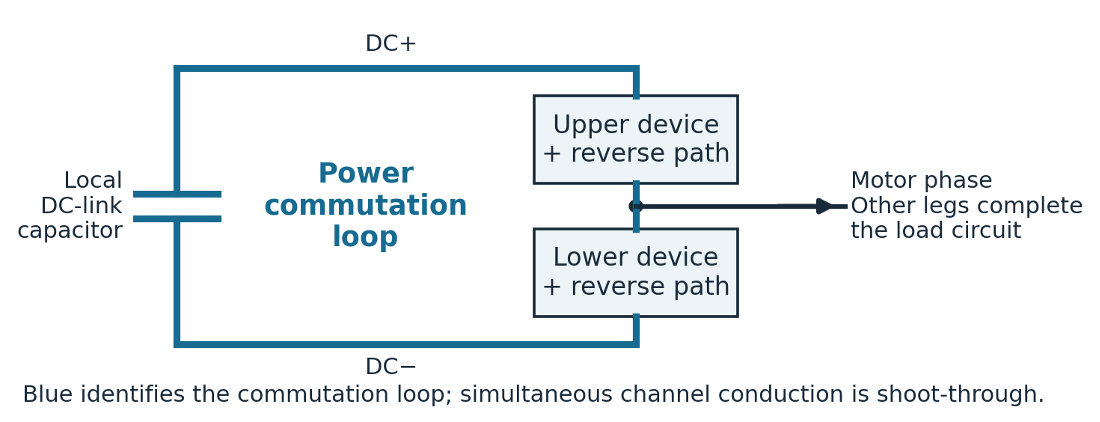
Figure 1. One half bridge in a motor inverter. During commutation, current changes rapidly in the highlighted paths. The motor’s current continues through the larger circuit containing the load. Each device block includes its applicable reverse-current path.
For example, current may initially flow through the lower device’s diode. When the upper transistor turns on, it takes over that current. Compare the circuit immediately before and after turn-on to identify which branch currents changed. The two transistor channels must avoid conducting simultaneously, which would connect the DC rails through them.
In the layout, place the local capacitor near the switching devices. Route the outgoing and returning current paths close together to reduce the loop inductance.
How the Gate Loop Shares Source Inductance with the Power Loop
The gate driver loop runs from the driver output through the gate resistor to the gate terminal, returning via the switch source connection. Figure 2 shows where power and gate loops intersect at the source lead.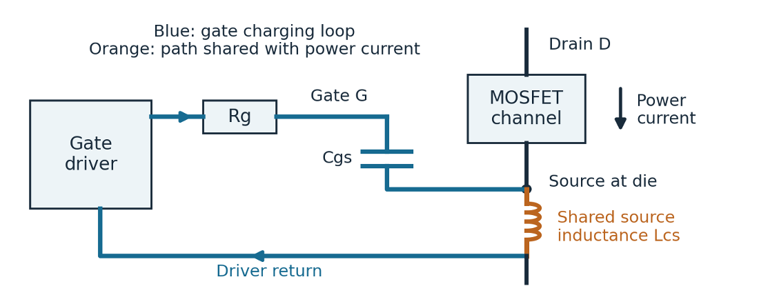
Figure 2. Gate charging current and power current both pass through the orange source connection. Its inductance may come from the transistor package, the PCB connection, or both. The drawing omits other gate capacitances and parasitic elements to show this shared connection clearly.
When power current changes in the shared source connection, the connection’s inductance produces a voltage. The transistor source then moves in voltage relative to the driver return terminal. Because the transistor responds to the voltage between its gate and source, this source-voltage movement changes what the transistor receives from the driver.
A dedicated Kelvin source connection gives the gate-driver return its own path to the transistor’s source. This reduces the source inductance shared with power current. Both source connections still join at the transistor die. Separately, a rapid change in drain voltage drives current through the gate-to-drain capacitance, Cgd, also called the Miller capacitance. That current can disturb the gate voltage. [1, 5, 6]
Worked Example: Calculating Voltage Overshoot from Loop Inductance
Assume the power commutation loop has 10 nH of inductance. During one switching transition, its current changes by 50 A in 0.1 µs. First calculate the current slope, then multiply that slope by the loop inductance to estimate the magnitude of the inductive voltage:
ΔIΔt = 50 A0.1 μs = 500 A/μs
|VL| = L × |ΔI/Δt| = (10 nH) × (500 A/μs) = 5 V
For a switching transition where this contribution adds to a 60 V DC bus, the first-order drain-to-source voltage estimate is 60 V + 5 V = 65 V.
If the inductive voltage adds to the 60 V DC bus during the transition, the first-order drain-to-source voltage estimate is 65 V. This estimate accounts only for the stated loop inductance and current slope. Ringing and other switching effects may raise the actual peak.
To investigate gate-voltage disturbance, calculate the voltage across the gate-loop inductance using the gate-current rate of change. Assess the shared source connection separately. Use its inductance and the rate of change of the current passing through that connection.
How to Model PCB Parasitics in Pre-Layout Inverter Simulations
Build a switching circuit model with one half bridge, its gate driver, a local DC-link capacitor, and an inductive load. Add an inductance to represent the power commutation loop. Add separate inductances for the gate loop and shared source connection. Keeping them separate lets you see which current produces each unwanted voltage.
Use device models that include the relevant transistor capacitances. Where a diode conducts, include its reverse-recovery behavior: after forward conduction, some diodes briefly carry reverse current as they turn off. Also include the DC-link capacitor’s series resistance and inductance. Omitting these parts can hide the ringing or voltage peaks you are trying to predict.
Run the simulation with several plausible values for each loop inductance. Repeat the comparison at the intended bus voltages, motor currents, and device temperatures. For each case, inspect drain-to-source voltage, gate-to-source voltage, and switching current. Once the PCB layout is available, obtain inductance values from extraction or measurement. Replace the early estimates and rerun the same operating cases.
How to Choose Gate Resistance and Dead Time from Switching Waveforms
Increasing the gate resistor usually slows the transistor’s switching transition. A slower current change can reduce the voltage generated by loop inductance. This may reduce overshoot and ringing enough to keep the transistor below its voltage rating.
The transistor may then spend longer carrying current while supporting voltage. During that overlap, it converts electrical energy into heat. Calculate the resulting switching power loss and check device temperature before accepting the larger resistor.
Next, check that one transistor has stopped conducting before the other turns on. Dead time creates a gap between their switching commands to allow that to happen. If the gap is too short, both transistor channels may conduct together and cause shoot-through. If the gap is too long, current spends more time in a diode or another reverse-conduction path. That can increase power loss and distort motor current.
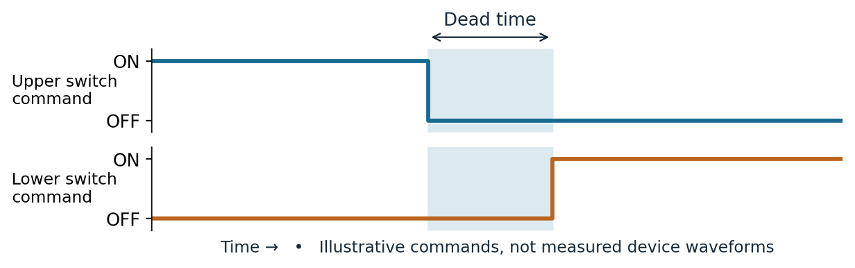
Figure 3. The upper-device turn-off command comes before the lower-device turn-on command. The gap between them is dead time. Each transistor responds after delays set by the driver, gate resistor, and device behavior. Check actual transistor conduction as well as the command timing.
Changing the gate resistor changes how quickly the transistor responds. Recheck dead time after each resistor change. Verify the actual transistor voltage and current at the intended temperatures and supply voltages. Also check both directions of motor current and the possible variation in driver timing.
If a larger resistor reduces overshoot but makes the device too hot, investigate the power-loop layout again. If turn-off has become too slow, revisit the driver settings and dead time as well.
You can now trace a voltage spike to a current loop and check how a gate-resistor change affects switching and heating. Use the checklist below whenever the transistor, driver, or PCB layout changes. Repeating the same checks makes it easier to compare revisions.
Inverter Switching Evaluation Checklist
- Trace the power commutation loop and gate loop for each half bridge. Mark any source connection shared by power current and gate-driver return current.
- Record DC bus voltage, motor current, and device temperature. List the resistance, inductance, and capacitance values assumed in the circuit model.
- Check the highest and lowest gate-to-source voltages against device limits. Check the drain-to-source voltage peak and calculate switching power loss.
- Verify that the upper and lower transistor channels avoid simultaneous conduction. Repeat for both current directions, operating extremes, and turn-off during a fault.
- Compare simulated transistor voltages and currents with measurements. Use probes fast enough to capture the transitions, keep probe connections short, and measure each voltage between the correct two terminals.
Connect PSpice Switching Simulation to PCB extraction
Use PSpice to simulate transistor voltage and current while varying the circuit parameters. Use Allegro X PCB Layout and Constraint Manager to implement the copper routing and design rules. [2]
To estimate the electrical behavior of the routed connections, Cadence documents an extraction workflow in Clarity 3D Layout and Clarity 3D Workbench. It produces interconnect resistance, inductance, capacitance, and conductance models, abbreviated RLCG. [3] Select model terminals, also called ports, at the connections where current enters and leaves the structure. Include the conductor that carries the return current. Then check that the extracted model is suitable for the switching simulation. A layout can pass its design rules while still having too much loop inductance for the intended switching speed.
Frequently Asked Questions About Inverter Switching Loops
Why does turning a MOSFET ON too fast cause ringing?
When a MOSFET switches quickly, the rapid changes in voltage and current can excite the inductance of PCB traces and package connections. That inductance interacts with transistor and circuit capacitances. Energy moves between the inductance and capacitance, producing voltage oscillations that decay as circuit resistance dissipates the energy.
First identify where the ringing appears: across drain and source, or across gate and source. Then inspect that circuit’s current path. Shorter connections and a smaller loop area reduce parasitic inductance. A suitable gate resistor can damp gate ringing or slow the transition, but check the resulting switching power loss and dead time before accepting the change.
How can I calculate the dead time to prevent shoot-through?
Start with the time needed for one transistor to stop conducting before the other begins conducting. Account for the driver’s propagation delays, transistor switching times, gate resistance, and timing tolerances. Use the slowest expected turn-off and fastest expected turn-on across the intended current, temperature, and driver-supply conditions. Include a timing margin, then verify that the transistor channels do not overlap in conduction in either switching direction.
For the RC delay circuit in the original question, the logic input thresholds also determine the delay; multiplying resistance by capacitance alone does not establish the actual dead time. If your driver inserts dead time internally, check its datasheet’s definition and operating conditions. Excessive dead time can increase body-diode or reverse-conduction power loss, so verify temperature as well as timing.
Do I connect grounds on a 4-pin MOSFET with kelvin source?
Route the gate-driver output return to the MOSFET’s Kelvin source pin using a dedicated, short connection. Route the power current through the power-source pin. Both pins connect to the source inside the transistor, but separate connections let the gate-driver return bypass much of the inductance carrying the power current. Joining the pins into the same high-current PCB path can defeat that benefit.
Follow the MOSFET and driver manufacturers’ connection diagrams. For a high-side MOSFET, the gate-driver output return follows that MOSFET’s source voltage at the switching node. It must not be treated as the negative DC rail.
Technical references
[1] Texas Instruments: Fundamentals of MOSFET and IGBT Gate Driver Circuits, SLUA618A
[2] Cadence: Allegro X Design Platform
[3] Cadence: Clarity quasi-static RLCG extraction workflow
[4] Texas Instruments, Delay and Dead Time in Integrated MOSFET Drivers, SLVAF84, September 2021. Source
[5] Infineon Technologies, Design of external passive components and layout measures to reduce Vgs ringing, October 2022. Source
[6] Infineon Technologies, Kelvin-Source Pin, manufacturer-accepted support response, September 7, 2021. Source
[7] Motor Controller Design: A System Level Guide From Requirements to Hardware Verification, v13. Project source 06. Sections 6, 9, and 11 cover gate drive, switching behavior, and PCB implementation.
[8] Infineon Technologies, Dead-time estimation for power MOSFETs in hard-switching applications, July 29, 2026. Source